


Welcome to CBSbutler Recruitment
Job search:
Your dream job is one click away
Field Service Engineer - UK&IRE
Production Engineer
Stress Engineer
Senior Events Manager
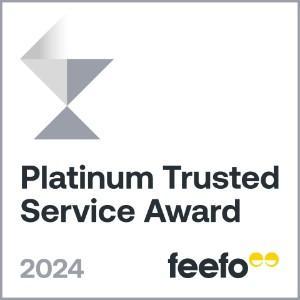
Awarding Winning
We are a multi-award-winning recruitment consultancy specialising in Engineering, BMS, Automation & Process Controls, Aviation & Aero, Manufacturing, ICT and Medical & Life Sciences appointments across global industries.
About CBSbutler
CBSbutler was established in 2003 with offices in the UK, there has never been a more exciting time to join us.

Candidate Hub
Visit our Candidate hub for the up to date tools and resources to get your dream job. From CV writing tips, to interview prep questions we got you covered.

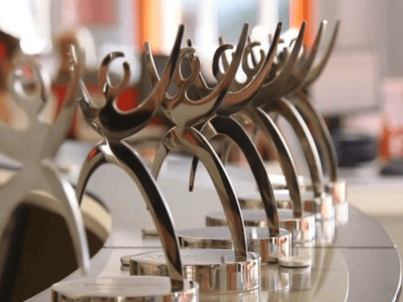
Our Awards Gallery
CBSbutler has received several awards for outstanding service by the Recruiter magazine, judged by our peers: The Best Engineering Recruitment Agency for 6 years & Best Agency in the UK – this number of wins has been unrivalled by any other Engineering/Technical recruitment agency in the UK.
Stay Updated


Client & Candidate Reviews
"An excellent company that can find you a job without delay. I honestly believe that CBSbutler is an outstanding organisation. It can find you a good job relative to your skill and experience within a short space of time."
Client review - AFC
"I strongly recommend CBSbutler’s service. They will work for us until we find right job. Very supportive and helpful."
Client - Service
"A credit to the recruitment industry! Fantastic communication throughout all stages of the hiring process. Thanks ever so much for the offer confirmation from Elsevier. This is a fantastic opportunity for me going forward for my career and the location could not be more perfect. The wife will be over the moon :) I would like to take the opportunity to thank you for getting in touch regarding this role and the smooth transition to a successful hire. You guys are a credit to your industry."
Client - Elsevier
"Alex Froude is excellent. He always responds to requests and queries promptly and completely."
Alex Froude - Very Responsive!
"I have worked with Dave Rowe for many years. Although he is not the only reason we work with CBSbutler, he is one of the primary reasons. I value quality and honesty over speed of response. I know that Dave always delivers the highest quality by taking the necessary time."
David Rowe - Aviation
"We appreciate and value the partnership and services relationship we have with CBSbutler."
Client
"The team at CBSbutler are professional, knowledgeable, and very approachable. I would recommend CBSbutler to other organisations."
Client - professional
"Amazing communication and also incredibly helpful. Always on hand to help and also very friendly. Bethan in particular was outstanding."
Bethan Conroy - M&LS
"It's been a pleasure working with Tom and CBSbutler over the last 18 months. Tom’s dedication and professionalism in supporting me as a contractor during this time has been really appreciated. Tom has always gone the extra mile and had my back during any contract negotiations, and I would fully recommend working with him."
Tom McParland
"Excellent and professional service. The consultant Bethan was very thorough in dealing with my application and she kept me regularly updated on each stage of process. What I found most helpful was the prep e-mail and publications she sent to me way ahead of my interview date. Also, I found her to be extremely polite, transparent and forthcoming re communications/feedback she got from company. All in all, Bethan has been one of the best agents I have interacted with and she was always willing to answer any questions I had at any time. We hope her efforts can be rewarded through an outstanding employee award."
Bethan Conroy - Royal Free Hospital
"It's been an absolute pleasure to work with Jonny, all the way through the last six-ish years. I can't thank you, Emma, and of course, the other teams in CBSbutler, enough for everything you’ve done for me since you joined CBSbutler, in fact, I’m pleased to have seen you rise to where you are now and I hope it continues for you."
Jonny Garrett & Emma Denmark
"Great communication, really professional with email or telephone conversations. Been a real pleasure to have worked with the company. If I needed an Agency to go to in the future this would be my first choice."
Client - Communication
"From the initial contract to being settled in a new role, Ciaran Digney communicated regularly and was provided in-depth customer knowledge which helped me no end."
Ciaran Digney
"Great service and agency staff, very professional in calls and communication always keeping me up-to-date on progress."